Experimental
Currently we are working on the following experimental aspects of the 2D materials:
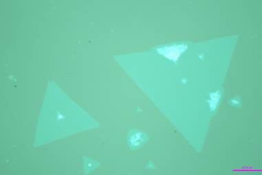
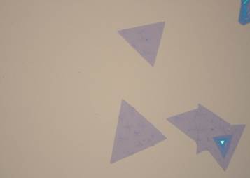
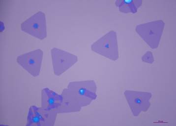
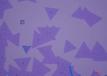
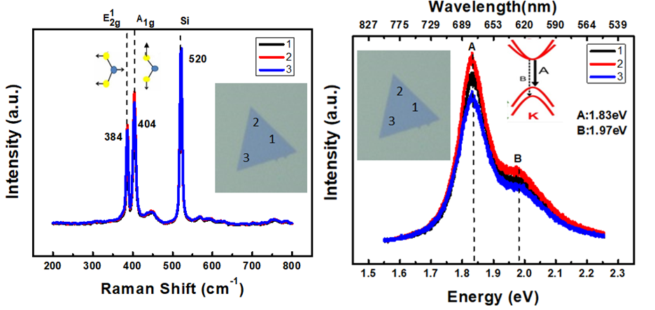
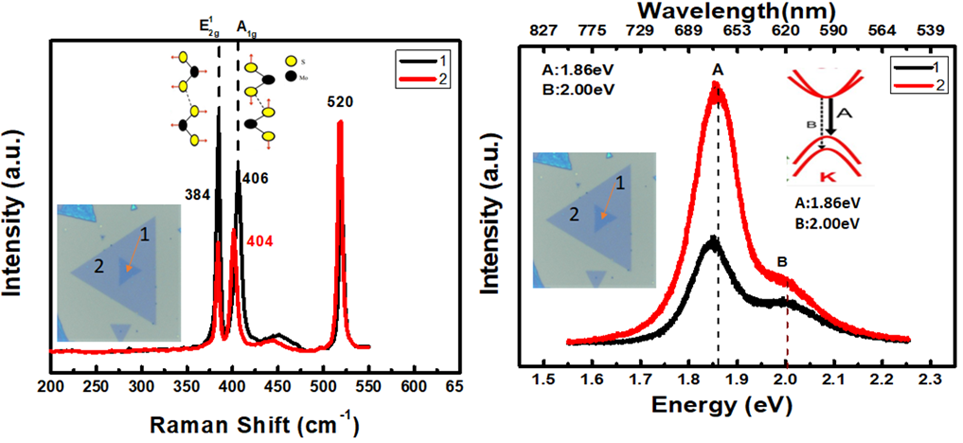
MoS2 grown using in our laboratory
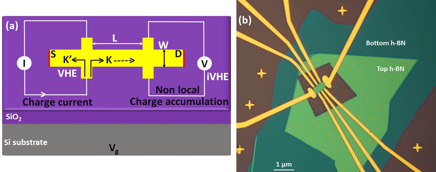
We are exploring in-plane and out of plane electrical transport in atomic layers and their heterostructures. Few device structures are:
- Top and back gated all 2D FETs, Hall bars and non-local measurements
